
Writing drivers for a Dot-Matrix LCD Display
January 14, 2018
- Read Part One about reverse engineering the LCD.
- Read about the inverting voltage multiplier I’m using to power the LCD.
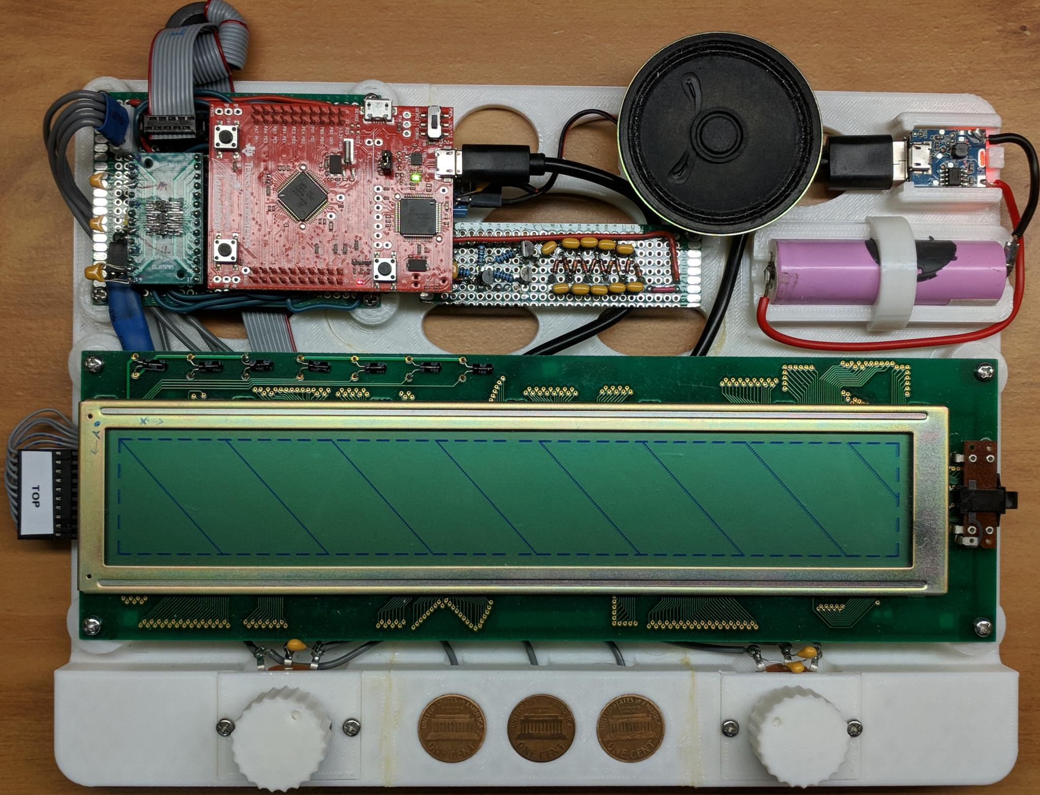
The previous post dealt with the LCD hardware and the specifics of the ICs. This post will focus on the driver code used to create the sequence of signals previously discussed. I’m using a TI dev board with the Cortex M4 core TM4C123GH6PM microcontroller.
Architecture
Before diving into the details of getting pixels to actually show up in the proper locations on the screen, let’s walk though a high level overview of how the driver is going to be set up.
- There will be two chunks of memory allocated as frame buffers. The two buffers will switch between being written to and being read from. This will be accomplished by using two pointers,
readBufferandwriteBuffer. - Sprites will be stored in row-column order, each row right padded to the nearest byte. Each bit will represent a single pixel. Zero meaning deactive (clear), and One meaning active (dark).
- Sprites will be loaded into the frame buffer currently pointed to by
writeBuffer. Upon loading the last sprite, the higher level code will let the driver know that the frame is complete. - A timer will trigger an interrupt and at each interrupt a single row of the
readBufferwill be loaded into the LCD controller ICs and latched out to display on the screen. - After loading the last row in a frame, a check is performed to determine if the pointers to the read and write buffers should be switched.
System Overview
The following digram shows a brief system overview limited to the portions of the system directly involved in using the LCD screen. In this post I’m going to focus on how data gets from memory (the buffer) to being displayed on the LCD. Future posts will delve into detail on how the sprites are stored and how the buffers get updated.
The modules involved are:
- main.c
- IO.c (IO.h)
- screen.c (screen.h)
- DisplayTests.c (DisplayTests.h)
The file main.c calls the appropriate initialization functions and then enters the infinite while loop. In the loop a check is performed to see if image data should be updated, that is, if a buffer is available to write to. If true, sprite states are updated and loaded into the current writeBuffer.

Main
The most relevant parts of main.c are shown below.
int main(void){

  DisableInterrupts();
  PLL_Init();
  IO_Init();
  EnableInterrupts();

  //Down the rabbit hole we go
  while(1){

    if(IO_Ready())
    {
      DisplayTests_DrawDiag();
      DisplayTests_DrawBorder();

      IO_UpdatesCompleted();
    }

  }
}
Input/Output (IO) module
The IO module has public functions declared in IO.h. The relevant public functions are shown below. The first three are called by main.c. The last, LoadSprite(), is called by DisplayTests.c.
void IO_Init(void);
bool IO_Ready(void);
void IO_UpdatesCompleted(void);
void IO_LoadSprite( const uint16_t xpos,
                    const uint16_t ypos,
                    const Sprite_t sprite );
Screen module
The screen module has public functions which are only called by IO.c. No other module is aware of its existence. The header file, screen.h, contains the declarations of these public functions as well as the screen width and screen height in pixels.
#define  SCREEN_W  480
#define  SCREEN_H  64

void Screen_Init(void);
void Screen_SetBufferIsFull(void);
bool Screen_IsBufferAvailable(void);
void Screen_ClearBuffer(void);
uint8_t * Screen_GetBuffer(void);
The Screen Driver
Alright, now that the overview is out of the way, let’s get into the meat of turning a bunch of ones and zeros into pixels on a screen.
Initialization
A few screen related constants, two arrays large enough to hold an entire screen of data, and two pointers to those arrays are initialized at the top of screen.c.
#define FRAME_REFRESH_HZ  11
#define LCD_REFRESH_HZ    44
#define BUFFER_SIZE          (SCREEN_W*SCREEN_H/8)

uint8_t ScreenBufferA[BUFFER_SIZE] = {0};
uint8_t ScreenBufferB[BUFFER_SIZE] = {0};
uint8_t *writeBuffer = NULL;
uint8_t *readBuffer = NULL;
There are five data signals which need to be handled.
- Data Clock (CP)
- Latch Clock (Load)
- Frame Clock (Row Data, DIO1)
- Column Data 1 (SDI)
- Column Data 2 (SDI)
These will use pins 4-0 on port F. The TM4C line of uCs has a feature which allows bits [9-2] of the address used to access a GPIO register to act as a mask, thus enabling atomic read and write operations on any combination of pins. This is known as “bit banding” or “bit-specific addressing.” See the following sections of the datasheet for more info:
- 10.2.1.2 Data Register Operation (p. 654)
- 2.4.5 Bit-Banding (p. 97)
and this webpage (ctrl-f for ‘bit-specific addressing’).
The first three signals will use PF1, PF2 and PF3 (respectively).
#define DataClk_PF1 (*((volatile unsigned long *)0x40025008))
#define LatchClk_PF2 (*((volatile unsigned long *)0x40025010))
#define FrameClk_PF3 (*((volatile unsigned long *)0x40025020))
The two serial data signals will always be written together, so a single mask will suffice.
#define SerialData_PF04 (*((volatile unsigned long *)0x40025044))
As an example, the address for accessing PF0 and PF4 simultaneously is calculated via:
Address \( =\textrm{Base_Address} + ((2^4 + 2^0)*4) \)
where the Base-Adress for the port F data register on the APB (Advanced Peripheral Bus) is 0x4002.5000. (Multiplying by 4 is equivilant to bit shifting left by 2.)
Now writing is as simple as:
DataClk_PF1 = (1<<1); //Make high
DataClk_PF1 = 0; //Make low;
SerialData_PF04 = (1<<4)|(1<<0); //Make both high
SerialData_PF04 = 0; //Make both low
SerialData_PF04 = (0<<4)|(1<<0); //Make PF4 low and PF0 high
These are great because they can’t effect any other pins than those intended, are way faster than the standard read-modify-write sequence, and because the operations are atomic (can’t be interrupted.)
The Init function
The Screen_Init() function has three jobs.
- Setup the GPIO pins needed for the LCD
- Setup the SysTick timer to trigger interrupts for sending data to the LCD
- Initialize the writeBuffer and readBuffer pointers
void Screen_Init(void){
  //////////////////////////////////////////////////
  //Enable GPIOs for connecting to LCD            //
  //////////////////////////////////////////////////
  SYSCTL_RCGC2_R |= (1<<5);                  // activate port F clock
  while((SYSCTL_PRGPIO_R & (1<<5)) == 0){;}  // Wait for clock to stabalize
  GPIO_PORTF_LOCK_R = 0x4C4F434B;            // unlock PortF PF0
  GPIO_PORTF_CR_R = 0x1F;                    // allow changes to PF4-0
  GPIO_PORTF_DIR_R    |=   ((1<<4)|(1<<3)|(1<<2)|(1<<1)|(1<<0)); // make PF4-0 out (1)
  GPIO_PORTF_AFSEL_R  &=  ~((1<<4)|(1<<3)|(1<<2)|(1<<1)|(1<<0)); // disable alt funct
  GPIO_PORTF_DR8R_R   |=   ((1<<4)|(1<<3)|(1<<2)|(1<<1)|(1<<0)); // can drive up to 8mA out
  GPIO_PORTF_DEN_R    |=   ((1<<4)|(1<<3)|(1<<2)|(1<<1)|(1<<0)); // enable digital I/O
  GPIO_PORTF_AMSEL_R  &=  ~((1<<4)|(1<<3)|(1<<2)|(1<<1)|(1<<0)); // no analog
  GPIO_PORTF_DATA_R   &=  ~((1<<4)|(1<<3)|(1<<2)|(1<<1)|(1<<0)); //set to zero


  //////////////////////////////////////////////////
  //Enable systick interrupts for writing to LCD  //
  //////////////////////////////////////////////////
  uint32_t sysTickReloadCount = (80000000/LCD_REFRESH_HZ/SCREEN_H);
  NVIC_ST_CTRL_R = 0;           // disable SysTick during setup
  NVIC_ST_RELOAD_R = sysTickReloadCount-1;     // reload value
  NVIC_ST_CURRENT_R = 0;        // any write to current clears it
  NVIC_SYS_PRI3_R = (NVIC_SYS_PRI3_R&0x00FFFFFF)|0x20000000; // priority 1
  NVIC_ST_CTRL_R = 0x07;  // enable with core clock and interrupts


  writeBuffer = ScreenBufferA;
  readBuffer = ScreenBufferB;
}
Public Interface
The following functions make up the public interface which is accessed by the IO.c module. The names should be fairly self explanatory.
uint8_t * Screen_GetBuffer(void)
{
  return writeBuffer;
}

void Screen_SetBufferIsFull(void)
{
  writeBufferIsFull = true;
  writeBufferAvailable = false;
}


bool Screen_IsBufferAvailable(void)
{
  return writeBufferAvailable;
}

void Screen_ClearBuffer(void)
{
  uint16_t i;
  for(i=0;i<BUFFER_SIZE;i++){
    writeBuffer[i]=0x00; //zeros correspond to the default clear pixel state
  }
}
Interrupt Handling
Each time the interrupt service routine is called, the row corresponding to the current value of rowIndex is loaded into the LCD. The value of rowIndex loops from zero up to SCREEN_H-1. A row stays active on the display until the next time the interrupt runs. The second part of the ISR only runs if the last row of a frame was just displayed, if the current frame has been displayed enough times, and if the new frame is ready. If all these conditions are met, then the read and write buffers are switched.
void SysTick_Handler(void){
  static const uint8_t minLcdUpdatesPerFrame = LCD_REFRESH_HZ/FRAME_REFRESH_HZ;
  static uint8_t rowIndex = 0;
  static uint8_t lcdUpdates = 0;

  PrintNextRow(rowIndex);
  rowIndex = (rowIndex+1)%SCREEN_H;

  if(rowIndex==0 and ++lcdUpdates>=minLcdUpdatesPerFrame and writeBufferIsFull)
  {
      SwitchBuffer();
      writeBufferAvailable = true;
      lcdUpdates = 0;
      writeBufferIsFull = false;
  }
}
static void SwitchBuffer(void)
{
  if(writeBuffer == ScreenBufferA)
  {
    writeBuffer = ScreenBufferB;
    readBuffer = ScreenBufferA;
  }
  else
  {
    writeBuffer = ScreenBufferA;
    readBuffer = ScreenBufferB;
  }
}
Printing a row
A few requirements
- The interrupt rate will be such that the entire LCD is refreshed at a rate of at least 40 Hz, that is (40Hz)*(number of rows). I found that below this rate there would visible flickering.
- The data clock must not exceed 3.3 MHz (as per the LCD driver IC datasheets)
- The width of a clock pulse must not be less than approx 80 ns (The datasheet says 100 ns, but in testing I found down to about 80 ns to be fine.)
Logical flow
The flowchart below shows the function PrintNextRow() and the functions it calls. The LCD is split into a left and right half so the first bit of the left half and the first bit of the right half get sent on the same falling edge of the data clock, etc… The falling edge of the latch clock tells the LCD ICs to take their data buffers and output them to their physical pins as high or low voltages. This signal also tells the IC controlling the rows to shift to the next row. The frame clock shifts in a new high value to the row IC which then gets shifted through each row by the latch clock signal until shifting off the last pin on the IC. This way the rows can be activated one at a time.

The following code is logically equivalent but has been modified from the simplest implementation to achieve the 3.3 MHz data rate.
- The “for each bit in a byte” loop has been unrolled
- The SendData() function has been integrated into the unrolled loop
These two changes drastically improved the data rate, actually getting over 5 Mhz. The delayns() is used to tune the data rate to close to 3.3 MHz as measured on a scope.
static void PrintNextRow(uint8_t rowIndex){

  uint8_t bytesPerRow,colIndex;
  uint8_t bufferByteLeft, bufferByteRight,bitValLeft,bitValRight;
  bytesPerRow = SCREEN_W>>3;// divided by 8 (bytes)

    for(colIndex=0;colIndex<(bytesPerRow>>1);++colIndex){
      bufferByteLeft = readBuffer[rowIndex*bytesPerRow+colIndex];
      bufferByteRight = readBuffer[rowIndex*bytesPerRow+colIndex+(bytesPerRow>>1)];

      DataClk_PF1 = (1<<1);
      bitValLeft = (bufferByteLeft&(1<<7))>>7;
      bitValRight = (bufferByteRight&(1<<7))>>7;
      SerialData_PF04 = ((bitValRight)<<0)|((bitValLeft)<<4);
      DataClk_PF1 = 0x00; //Clocks in data on falling clock edge
      delayns();

      DataClk_PF1 = (1<<1);
      bitValLeft = (bufferByteLeft&(1<<6))>>6;
      bitValRight = (bufferByteRight&(1<<6))>>6;
      SerialData_PF04 = ((bitValRight)<<0)|((bitValLeft)<<4);
      DataClk_PF1 = 0x00; //Clocks in data on falling clock edge
      delayns();

      DataClk_PF1 = (1<<1);
      bitValLeft = (bufferByteLeft&(1<<5))>>5;
      bitValRight = (bufferByteRight&(1<<5))>>5;
      SerialData_PF04 = ((bitValRight)<<0)|((bitValLeft)<<4);
      DataClk_PF1 = 0x00; //Clocks in data on falling clock edge
      delayns();

      DataClk_PF1 = (1<<1);
      bitValLeft = (bufferByteLeft&(1<<4))>>4;
      bitValRight = (bufferByteRight&(1<<4))>>4;
      SerialData_PF04 = ((bitValRight)<<0)|((bitValLeft)<<4);
      DataClk_PF1 = 0x00; //Clocks in data on falling clock edge
      delayns();

      DataClk_PF1 = (1<<1);
      bitValLeft = (bufferByteLeft&(1<<3))>>3;
      bitValRight = (bufferByteRight&(1<<3))>>3;
      SerialData_PF04 = ((bitValRight)<<0)|((bitValLeft)<<4);
      DataClk_PF1 = 0x00; //Clocks in data on falling clock edge
      delayns();

      DataClk_PF1 = (1<<1);
      bitValLeft = (bufferByteLeft&(1<<2))>>2;
      bitValRight = (bufferByteRight&(1<<2))>>2;
      SerialData_PF04 = ((bitValRight)<<0)|((bitValLeft)<<4);
      DataClk_PF1 = 0x00; //Clocks in data on falling clock edge
      delayns();

      DataClk_PF1 = (1<<1);
      bitValLeft = (bufferByteLeft&(1<<1))>>1;
      bitValRight = (bufferByteRight&(1<<1))>>1;
      SerialData_PF04 = ((bitValRight)<<0)|((bitValLeft)<<4);
      DataClk_PF1 = 0x00; //Clocks in data on falling clock edge
      delayns();

      DataClk_PF1 = (1<<1);
      bitValLeft = (bufferByteLeft&(1<<0))>>0;
      bitValRight = (bufferByteRight&(1<<0))>>0;
      SerialData_PF04 = ((bitValRight)<<0)|((bitValLeft)<<4);
      DataClk_PF1 = 0x00; //Clocks in data on falling clock edge
    }
    if(rowIndex==0)
      FrameClock();
    else
      LatchClock();
}
//Latch Clock: LatchClk_PF2
static void LatchClock(void){
  unsigned long i=17; //specific number doesn't matter
  LatchClk_PF2 = (1<<2);
  i=i/i; //Delay enough to keep peak at least ~80ns wide
  LatchClk_PF2 =  0x00;
}

//DIO1: FrameClk_PF3
static void FrameClock(void){
  FrameClk_PF3 =   (1<<3);
  LatchClock();
  FrameClk_PF3 =  0x00;
}

static void delayns(void){
  unsigned int i;
  i=i/i/i;
}
Ideas for the Future
The code I have now is working quite well, but I think I could utilize a dual SPI setup to do the actual sending of each row. I believe there are some microcontrollers which can send multiple streams of data on a single SPI peripheral, but I don’t believe the one I’m using can. But I might be able to use two SPI peripherals and have them share a single clock.
If I get SPI working I’d also like to utilize DMA for transferring data to the SPI peripheral.